ICEA convenes inaugural India fabless semiconductor design acceleration workshop at IIT Bombay
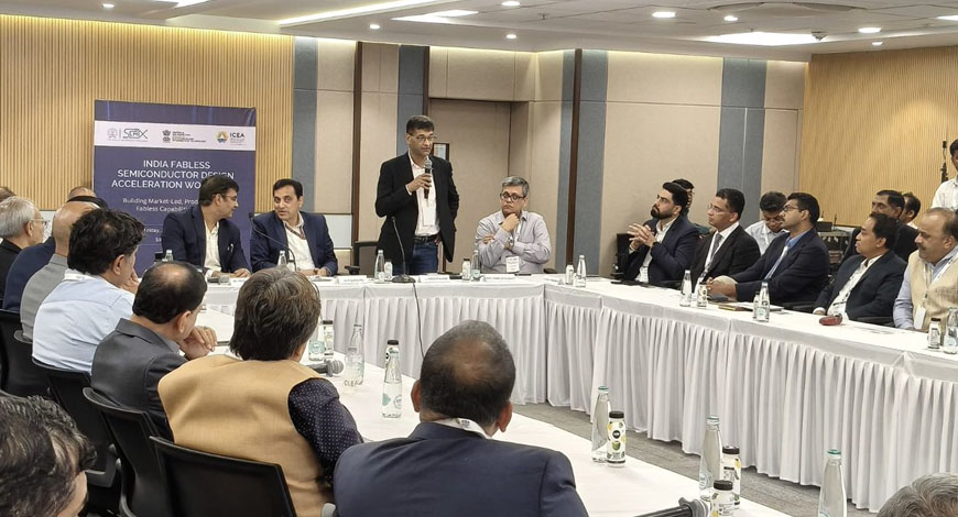
On March 2, 2026, the India Cellular & Electronics Association (ICEA), in collaboration with the Indian Institute of Technology (IIT) Bombay, hosted the inaugural India Fabless Semiconductor Design Acceleration Workshop. This event, titled “Building Market-Led, Product-Driven Fabless Capabilities in India,” took place at the IIT Bombay campus and aimed to enhance the semiconductor design ecosystem in the country.
Workshop Overview
The full-day workshop featured a Leadership Roundtable focused on the ambitious goal of establishing 500 fabless semiconductor companies in India. It included targeted track sessions and concluded with a Blueprint discussion aimed at outlining actionable steps for participants.
Participants and Stakeholders
More than 60 senior participants attended the workshop, representing a diverse range of stakeholders including:
- Government officials
- Semiconductor design companies
- Fabless startups
- Venture capital funds
- Incubators
- Academia
- Ecosystem institutions
Objectives of the Workshop
The primary objective of the workshop was to foster structured and outcome-driven discussions on strengthening India’s semiconductor product design ecosystem. The event marked the beginning of a series of engagements that ICEA plans to convene under the ICEA Semiconductor Product Design Leadership Forum. This initiative aims to:
- Synergize and converge knowledge within the semiconductor industry
- Align market demand with product development
- Facilitate capital formation for semiconductor startups
- Create effective execution pathways for product development
Significance of Fabless Semiconductor Companies
Fabless semiconductor companies play a crucial role in the global electronics supply chain. They focus on designing and selling hardware devices while outsourcing the manufacturing process to semiconductor foundries. This model offers several advantages:
- Cost Efficiency: Reduces the need for heavy capital investments in manufacturing facilities.
- Focus on Innovation: Allows companies to concentrate on design and innovation, leading to faster product development cycles.
- Flexibility: Enables companies to adapt quickly to market changes and technological advancements.
Future Engagements and Initiatives
The workshop at IIT Bombay is just the first in a structured series of events that ICEA will organize. Future workshops and discussions will aim to:
- Enhance collaboration between academia and industry
- Promote research and development in semiconductor technologies
- Encourage investment in the semiconductor sector
- Support the growth of startups in the fabless design space
Conclusion
The inaugural India Fabless Semiconductor Design Acceleration Workshop at IIT Bombay represents a significant step towards building a robust semiconductor design ecosystem in India. By bringing together key stakeholders, ICEA aims to create a collaborative environment that fosters innovation and growth in the semiconductor sector.
Note: The information presented in this article is based on the latest updates and developments in the semiconductor industry as of March 2026.